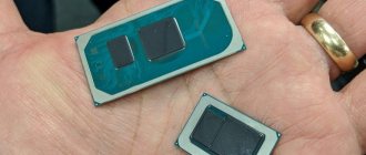
In September 2020, Apple introduced three new smartphones: iPhone 11, iPhone 11 Pro and iPhone 11 Pro Max. Their main feature, of course, turned out to be cameras, the general operating principles of which we discussed in a separate article. However, the processor of the new products also deserves special attention. Their “heart” was the Apple A13 Bionic, which was created using a 7-nanometer technological process. The manufacturer is proud of this figure, because not all competitors have reached it. But Xiaomi Redmi 8 Pro has a MediaTek Helio G90T chip. It’s all 12 nm, and there’s definitely nothing to boast about here...
The best Telegram channel about technology (possibly)
In general, in the world of high technology there is nothing faster than the most agile chips - processors. They can process billions of operations per second, and so much incredible technology goes into their production that it’s even creepy. Microprocessors went into mass production in the 90s of the last century. Since that time, they have experienced several stages of development, the apogee of which was the beginning of the 21st century. It was then that manufacturers discovered all the basic properties of silicon, and this made it possible to obtain maximum efficiency at minimal cost.
Today, the pace of processor development is rapidly falling. Silicon technology is rapidly approaching its physical limits. Yes, their frequencies are still increasing, but their operating efficiency is stagnating. We will talk about this in the context of smartphones and not only in this article.
What is each microprocessor basically?
Each microprocessor is a special integrated circuit that is located on a microscopic silicon chip. This material is used only because it has the properties of semiconductors: it conducts electricity faster than dielectrics and slower than metals. It can be made both an insulator, which stops the movement of charges, and a conductor, which lights up a green light for them. This parameter can be controlled using special impurities.
Inside the microprocessor there is room for millions of transistors, which are connected by incredibly thin conductors. Aluminum, copper and other materials are used for their production - they are designed to digest information. They make up internal buses, which give the processor the ability to work with mathematical and logical operations, as well as control the rest of the device’s chips in general.
One of the most important parameters of microprocessor quality has always been the operating frequency of its crystal. It is she who determines the number of actions that can be performed in the allotted time - this depends on how quickly the transistors can transition from a closed state to an open state. This is not least influenced by the production technology of silicon wafers, the main component of processors. The smaller they are, the more often you can overclock their frequency to higher values.
The manufacturing process used to manufacture microprocessors affects their size. If you cut off the number of nanometers that everyone is talking about today, you can reduce the size of the chip itself. This will make it not only faster, it will generate less heat and use less energy. These indicators have always been very important in full-fledged computers, but now they almost take first place in modern smartphones.
What does "nm" actually mean?
CPUs are made using photolithography, where an image of the CPU is etched onto a piece of silicon. The exact method of how this is done is usually called process node and is measured by how small the transistors can be made by the manufacturer.
Because smaller transistors are more power efficient, they can perform more calculations without overheating, which is usually the limiting factor for processor performance. It also allows for smaller die sizes, which reduces costs and can increase density for the same size, meaning more cores per die. 7nm is actually twice as dense as the previous 14nm node, allowing companies like AMD to produce 64-core server chips, a significant improvement over their previous 32 cores (and Intel's 28 cores).
However, it is important to note that while Intel is still using the 14nm node and AMD is set to release its 7nm processors soon, this does not mean that AMD will be twice as fast. Performance does not correspond to the size of the transistor, and at such small scales these numbers are no longer as accurate. How each semiconductor manufacturing facility measures can vary from one to another, so it's best to think of them more as marketing terms used to segment products rather than precise measurements of power or size. For example, Intel's upcoming 10nm node is expected to compete with TSMC's 7nm node, even though the numbers don't match.
What stages do processors go through during production?
Even if you believe Wikipedia, the production of processors can be divided into one and a half dozen stages. We decided to briefly describe each of them precisely so that it becomes clear how complex this process is. In reality, it is even more intricate, believe me.
1. Mechanical processing. At this stage, the manufacturer prepares conductor plates with a certain geometry and crystallographic orientation, which cannot differ from the standard by more than 5%. The class of surface cleanliness also deserves special attention.
2. Chemical treatment. As part of this stage, all the smallest irregularities that were created during machining are removed from the surface. For this, as well as to obtain the necessary nuances of the form, plasma-chemical methods, as well as liquid and gas etching, are used.
3. Epitaxial growth. In this case, a layer of semiconductor is added - the deposition of its atoms onto the substrate. It is at this stage that a crystalline structure is formed, similar to the structure of the substrate, which often serves only as a mechanical carrier.
4. Obtaining a disguise. To protect the semiconductor layer from subsequent penetration of impurities, a special protective coating is added to it at this stage. This occurs through oxidation of the silicon epitaxial layer, which is made possible by high temperature or oxygen.
5. Photolithography. At this stage, the necessary relief is created on the dielectric film. If up to this point in this paragraph of the article you have understood little at all, then our task is completed - you have realized how difficult it is to create a processor, and you can move on to the next point.
6. Introduction of impurities. Here we are, of course, talking about electrically active impurities, which are needed for the formation of insulating areas, as well as electrical transitions, the sources of which can be solid, liquid and gaseous substances. For this, the diffusion method is used.
7. Obtaining ohmic contacts. In addition, at this stage, passive elements are also created on the plate. This is done by using photolithographic processing on the surface of the oxide, which covers the areas of successfully formed structures.
8. Adding layers of metal. At this stage, the future processor receives several additional layers of metal, the total number of which can vary greatly and depends on its level. Between it you need to place a dielectric, in which there are through holes.
9. Surface passivation. To properly test a crystal, you need to clean it as much as possible from any possible contaminants. This most often occurs in deionized water in hydromechanical or brush washing units.
10. Plate testing. For this purpose, probe heads are usually used, which are installed on special installations used for sorting wafers. By the way, until this very moment they are in a state uncut into separate parts.
11. Plate separation. At this stage, the wafer is mechanically separated into individual crystals. Nowadays they do this not only because of convenience, but also because of maintaining electronic hygiene. Within its framework, there should be a critically small amount of dust in the air, and during the cutting process it will appear.
12. Crystal assembly. At this stage, the finished crystal is packaged in a special case, which is subsequently sealed. Here all the necessary pins that are needed for its further use are also connected to it - this is an almost ready-made chip.
13. Measurements and tests. At this stage, the chip is checked for compliance with the specified technical parameters. Yes, even in such a precise and high-tech production, defects occur, which increases with the complexity of the task. Hence the rather high price.
14. Control and labeling. These are the final couple of steps in chip production. In this case, they are checked again, then a special protective coating is applied to them, and they are also packaged in order to deliver the finished product to a specific customer.
Ruin of production
The chip consists of many transistors that act as switches. For many decades, progress in integrated circuits has followed Moore's law, in which the transistor density on a device doubles in 18 to 24 months.
In a similar rhythm, manufacturers introduced new technological processes with higher transistor density, which allowed the industry to reduce the cost of chips in terms of the number of transistors. At each process technology, manufacturers scaled transistor specifications by a factor of 0.7, allowing the industry to increase productivity by 40% with the same power consumption and half the area.
The integrated circuit industry followed this formula and flourished. Since the 1980s, it has paved the way for fast PCs at falling prices.
By 2001, there were at least 18 manufacturers with fabs where they could produce chips at 130 nm, which was the cutting-edge process at the time, according to IBS. Also at that time, several more new manufacturers appeared, making custom chips in other people's factories. In addition, the practice was to produce chips for laboratories that developed them, but did not have their own production.
By the end of the decade, production costs and technical processes skyrocketed. Unable to cope with rising prices, many chip manufacturers switched to the fab lite model. They produced some chips in-house and outsourced the rest.
Over time, fewer and fewer chip makers made cutting-edge devices in-house. Some completely got rid of production or left this business.
However, in the 2000s, the silicon workshop business model emerged. The workshops lagged behind Intel and other companies in technology, but gave engineering companies access to a variety of processes.
The next big change happened at 20 nm, when traditional planar transistors hit a wall and encountered the short-channel effect. In response, Intel moved to the next generation of transistor technology, finFET, at 22 nm in 2011. Workshops have switched to finFET at 16/14 nm.
finFETs have several advantages over planar transistors.
“In this design, the entire transistor is pulled vertically so that the channel rises above the substrate, and the valve wraps around three sides of the fin. The increased valve contact area allows for better control of leakage current,” write Matt Cogorno and Toshihiko Miyashita of Applied Materials. Cogorno is the director of global product management, and Miyashita is the chief technology officer.
FinFETs are also more complex devices; they are more difficult to produce and scale to each subsequent technological process. As a result, the cost of R&D has skyrocketed. So now the rhythm of a full process change has increased from 18 months to 2.5 years or more.
Integrated circuit prices also continue to rise. The cost of developing a 28 nm planar device ranges from $10 million to $35 million, according to Gartner. By comparison, the cost of designing a 7 nm system on chip (SoC) ranges from $120 million to $420 million.
“The cost of development is highly dependent on the complexity of the SoC,” said Samuel Wang, an analyst at Gartner. – Two-thirds go to chip development. The rest is the development of submarines, the cost of masks and improving the yield. Over time, the cost of design also falls.”
However, price trends have changed the landscape of the integrated circuit world. Over time, fewer and fewer companies can afford to pay for the design of chips for the most advanced technological processes. Many of them rely on workshops for production.
Fewer customers coupled with rising production costs have impacted the landscape of workshops producing advanced chips. For example, there are five manufacturers/workshops left in the 16/14 nm market: GlobalFoundries, Intel, Samsung, TSMC and UMC. SMIC also works with finFETs on the 14nm process.
And at 7 nm another transition occurred. Technological processes and production costs continued to rise, and the return on investment was already in question. As a result, GlobalFoundries and UMC stopped trying to develop a 7 nm process technology last year. Both companies continue to operate in the 16/14 nm market.
In an attempt to evolve further, Samsung and TSMC are racing full speed toward the 7 nm milestone and beyond. After several delays, Intel plans to launch production at 10 nm in mid-2019, and at 7 nm by 2021. SMIC, meanwhile, is not promising any timelines.
But not all workshop clients require advanced technical processes. There is a thriving market for 28nm chips.
“It all depends on the characteristics of the product,” said Gartner's Weng. – Some products require maximum performance. Developers may still use outdated technical processes. And chips for applications that do not require high performance can operate on N-1 and N-2 technical processes.”
Others echo him.
“How many companies can economically afford the latest silicon today? Their number is decreasing. In markets that require extremely high performance, this need will always exist. But in the supply chain, in terms of volume, there is a rift in the middle. The most demanding customers require 7, 5, and perhaps someday 3 nm processes. But everyone else has slowed down a little,” said Walter Ng, vice president of business management at UMC.
But in certain cases there is a need for the most advanced chips - these are servers and smartphones. There is also a sea of new AI chip startups emerging. Many companies are designing chips for machine learning and deep learning.
“No one disputes that the need to calculate something 10 times faster than today will always be commercially useful and competitive, even in non-technical markets. All these unique achievements of deep learning technology are evidence of this. There is literally no end in sight to the demands for more and more computing power,” said Aki Fujimura, director of D2S.
“Computing demand has seen several major shifts, first with GPUs and later with deep learning,” Fujimura said. – Deep learning is a massive technology for finding suitable patterns, and training neural networks is a problem of sequential optimization. Now that the world has come up with a mechanism to process huge amounts of data and turn it into useful information in the form of a program capable of logical conclusions, the number of calculations required is growing along with the amount of data available. And as the amount of data in all areas grows exponentially, the requirements for computing power are guaranteed to increase significantly, at least in the field of deep learning.”
Whether AI chips require process technology at 5nm and beyond remains unclear, but demands for increased computing power certainly exist. But migration to these technical processes does not become an easier or cheaper process.
Process Downsizing Timeline
'70s:
- 3 microns - Zilog achieved this technological process in 1975, Intel - in 1979.
'80s:
- 1.5 microns - Intel reduced the process technology to this level in 1982;
- 0.8 microns - Intel level in the late 1980s.
'90s:
- 0.6-0.5 microns - Intel and IBM were at this level in 1994-1995;
- 350 nm - Intel, IBM, TSMC by 1997;
- 250 nm - Intel, 1998;
- 180 nm - Intel and AMD, 1999.
'00s:
- 130 nm - Intel and AMD reached this level in 2001–2002;
- 90 nm - Intel in 2002–2003;
- 65 nm - Intel in 2004–2006;
- 45–40 nm - Intel in 2006–2007;
- 32–28 nm - Intel in 2009–2010;
- 22–20 nm - Intel in 2009–2012;
'10th:
- 14–16 nm - Intel has launched production of such processors by 2015;
- 10 nm - TSMC made such processors already in 2016, and Samsung in 2020;
- 7 nm - TSMC, 2020;
- 6 nm - TSMC only announced this process technology in 2019;
- 5 nm - TSMC began testing this process technology in 2019;
- 3 nm - Samsung promises to make processors with this technological process by 2021.
Where does Apple get 5 nanometers?
Apple is engaged exclusively in the development of its processors, but not in their production. Its own specialists took part in the work on the A14, and the Taiwanese company TSMC will produce it, due to Apple’s lack of factories for production.
In terms of topology, A14 has no analogues in the world yet
TSMC fully mastered the 5-nanometer process in 2020, and it became one of the first companies ready to produce the corresponding chips. So far, only Samsung competes with it in this regard.
- Russia's first IT marketplace Market.CNews for your business. With IT service prices from hundreds of providers
- Short link
The fewer nanometers in the technological process, the:
Higher operating speed. In the mobile processor segment, the fastest today is the Apple A13 Bionic, which is made using a 7-nanometer process technology - this is the fastest value available in the commercial sector today. A reduction in process technology is often followed by an increase in productivity. Today it is vitally needed for using neural networks, for augmented reality, and working with graphics anywhere and at a convenient time. What can I say, with the release of Apple Arcade we are expecting a boom in mobile games, and for them the processor is also important.
Lower heat generation. Today we focus on mobile devices. There is an opinion that talking about processor temperatures is not so relevant in smartphones, but this is a big mistake. Under heavy load, processors get hot. If the temperature becomes critical, they reduce the speed of their work - this is called throttling. To avoid this, you need to make the case thicker, think about additional heat removal, and so on. When using a more advanced technological process, the number of such problems is noticeably reduced.
Less energy consumption. After all, process reduction is very important for increasing battery life. That is why, when assessing the battery capacity of an inexpensive Android smartphone, you do not need to compare it with the corresponding indicator in the iPhone and other flagships. Even with a much larger battery capacity, the device may not work as long as we would like. The same Xiaomi Redmi 8 Pro with a processor made using an outdated technological process (12 nm) does not please with autonomy even with a fairly large battery.
In conclusion, I repeat - when choosing a new smartphone, you should not least look at the technological process of the chipset. Progress surpassed the 12 nm bar back in 2020, so in 2019 this figure even looks kind of funny.